Editor’s Note
This article reports on the historic first jewelry export consignment from Mumbai to the UK under the India-UK CETA, part of a broader national campaign involving key cities.
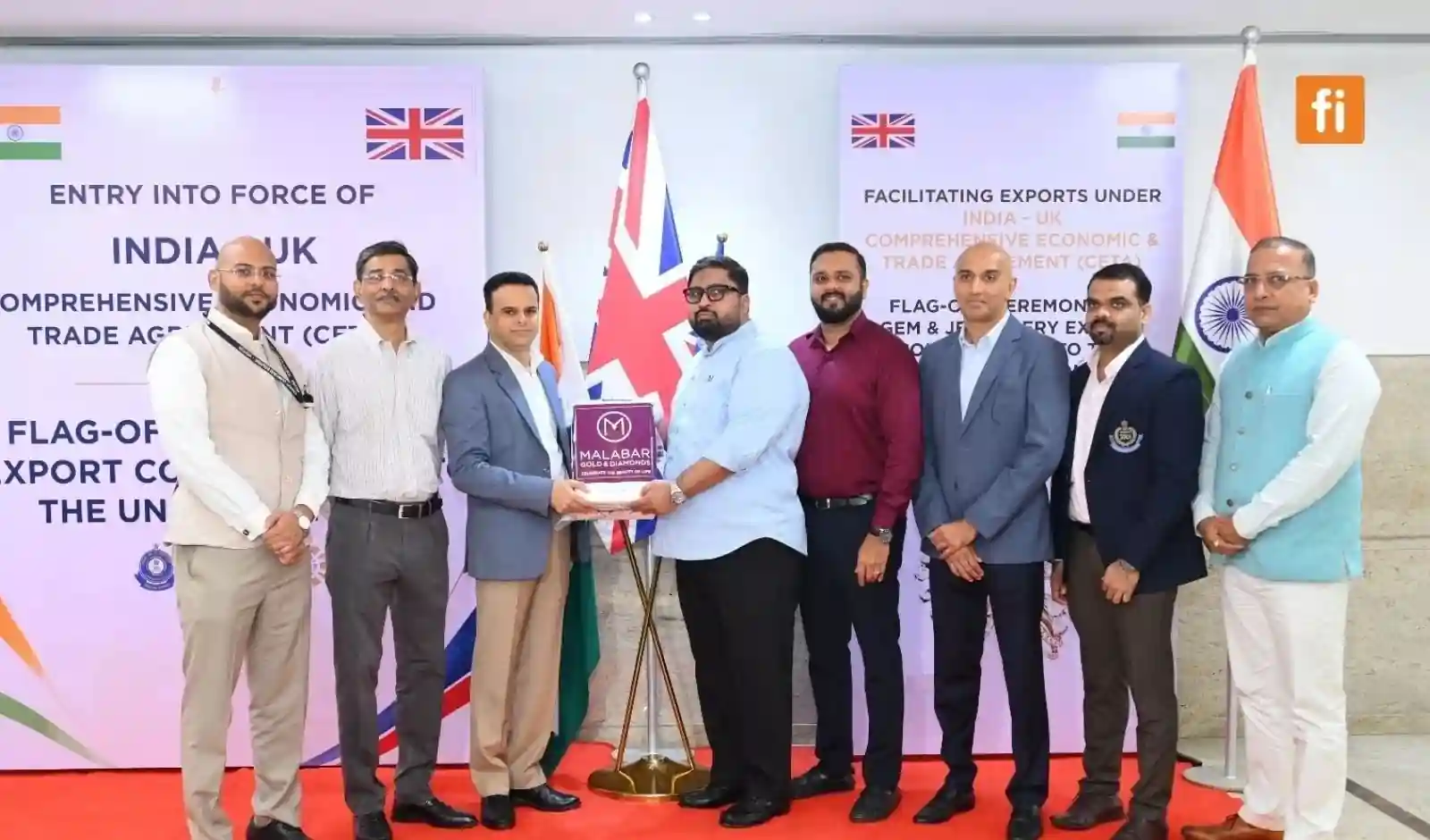
The first jewelry export consignment from Mumbai, India’s financial capital and leading gems and jewelry export hub, to the United Kingdom under the India-UK Comprehensive Economic and Trade Agreement (CETA) has been flagged off. This is considered a historic achievement for India’s gems and jewelry industry.
The flag-off event in Mumbai is part of a national campaign that also saw first jewelry consignments sent to the UK from Delhi, Surat, Jaipur, Chennai, and Kolkata. Collectively, jewelry worth a total of US$10 million (1 crore US dollars) was exported from these cities.
The Mumbai events were held at two major export centers: the Bharat Diamond Bourse (BDB) and the SEEPZ Special Economic Zone (SEEPZ-SEZ), both playing crucial roles in India’s gems and jewelry exports. At the Bharat Diamond Bourse event, Mumbai’s Commissioner of Customs Santosh Kumar, Deputy Director General of Foreign Trade (DGFT) Vishwajeet Chimankar, and Vice Chairman of the Gem and Jewellery Export Promotion Council (GJEPC) Shaunak Parikh were present. Major exporters including Malabar Gold & Diamonds, Shree Ramkrishna Exports, and Venkatesh Jewellers participated. At the SEEPZ-SEZ event, Development Commissioner Dnyaneshwar Patil, Joint Development Commissioner Mayur R. Mankar, GJEPC’s Bharat Ghori, SEEMA Vice President Vijay Gujarati, and SGJMA President Adil Kotwal were present. Key exporters such as Kama Jewellery, Suashish Diamonds, Goldstar Jewellery, Supergems Jewellery, and Zenstar Jewellery also took part.
With the implementation of the India-UK CETA, the Indian gems and jewelry industry will gain significant advantages in the UK market. Under the agreement, the import duty of up to 4% on Indian jewelry will be completely eliminated, granting Indian exporters zero-duty market access from day one. This will provide Indian companies with a competitive edge in the US$4 billion UK jewelry import market. The industry expects this to create new opportunities for exports, investment, and employment.
Mumbai’s Commissioner of Customs Santosh Kumar stated that the India-UK CETA brings new opportunities for Indian exporters, enhancing their competitiveness in the UK market.
SEEPZ Development Commissioner Dnyaneshwar Patil called the India-UK Free Trade Agreement (FTA) a historic opportunity for the gems and jewelry industry. He noted that the elimination of the 4% import duty on Indian jewelry in the UK will make Indian products more competitive.
GJEPC Chairman Kirit Bhansali stated that the India-UK CETA marks the beginning of a new era for the Indian gems and jewelry industry. He expressed gratitude to Prime Minister Narendra Modi and the Indian government for this historic agreement.
GJEPC Vice Chairman Shaunak Parikh highlighted Mumbai’s long-standing role as a major center for India’s gems and jewelry exports.
Industry experts believe that the India-UK CETA will particularly benefit Maharashtra’s gems and jewelry industry, promoting better market access, value-added manufacturing, job creation, skill development, and MSME participation. Mumbai’s strong diamond trading, jewelry manufacturing, export, and logistics network will play a crucial role in India’s export expansion. The dispatch of the first duty-free jewelry consignment to the UK signals that the Indian jewelry industry is ready to further strengthen its presence in the global market.
