Editor’s Note
This article explores the advanced applications of Chemical Vapor Deposition (CVD), a cornerstone technique in microfabrication. It highlights how modern CVD processes enable the precise synthesis of both inorganic 2D materials and high-purity polymer thin films, pushing the boundaries of semiconductor manufacturing and materials science.
The Chemical Vapor Deposition (CVD) process is often used in manufacturing semiconductors and producing thin films. In recent years, CVD synthesis has reached new heights with the precise manufacturing of both inorganic thin films of 2D materials and high-purity polymeric thin films that may be conformally deposited on various substrates.
CVD is widely used in microfabrication techniques to deposit materials in various forms, including polycrystalline, monocrystalline, amorphous, and epitaxial. These materials include silicon (dioxide, carbide, nitride, oxynitride), carbon (fibers, nanofibers, nanotubes, diamond, graphene), fluorocarbons, filaments, tungsten, titanium nitride, and various high-k dielectrics.
Thin-film deposition is a vital step in manufacturing integrated circuits (ICs). The most common approach for thin-film growth is CVD. Precursors and reactants are combined in a process chamber before being delivered in a steady state to form a film on the wafer in CVD.
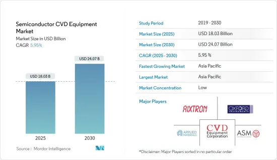
The Semiconductor CVD Equipment Market size is estimated at USD 18.03 billion in 2025, and is expected to reach USD 24.07 billion by 2030, at a CAGR of 5.95% during the forecast period (2025-2030).
Increasing demand for microelectronics-based consumer products, resulting in the faster growth of the semiconductor, LED, and storage device industry and strict regulations on the use of Cr6 for electroplating are primarily driving the growth of the CVD equipment market.
Precursor gases (typically diluted in carrier gases) are supplied into the reaction chamber at around ambient temperatures in semiconductor chemical vapor deposition equipment. They react or break down when they pass across or come into touch with a heated substrate, generating a solid phase that is deposited on the substrate. The temperature of the substrate is important because it can influence the reactions that occur.
Because these technologies have the potential to disrupt and drive the Internet of Things market, governments and stakeholders in emerging economies are closely watching developments in the microelectronics industry. As the adoption of virtual reality and augmented reality gadgets increases, microelectronics research and development is also likely to increase to address impending bandwidth constraints.
The COVID-19 outbreak impacted the entire semiconductor and chip manufacturing market from both demand and supply sides. Nationwide semiconductor plant shutdowns and closures have further spurred the trend of supply shortages. However, these impacts are short-term and are likely to have a temporary effect on the demand for CVD technology. Furthermore, precautionary measures by governments worldwide to support the automotive and industrial sectors could help revive growth in the foundry industry.
Rising sales of microelectronics and consumer electronics are expected to boost demand for semiconductor ICs during the forecast period. However, the demand for semiconductor ICs is expected to enhance the production capacity of semiconductor device manufacturers, potentially increasing demand in the chemical vapor deposition market.
Integrated Device Manufacturers (IDMs) include logic, optoelectronics, sensors, discrete components, and others (excluding memory manufacturers). Integrated Device Manufacturers manufacture and sell integrated circuits (ICs). A typical IDM owns its branded chips, designs them in-house, and manufactures them in its own fabrication plants. While IDMs pursue node miniaturization from 10nm to 5nm and even 3nm, other manufacturers are abandoning planar architectures in favor of sophisticated three-dimensional (3D) structures for logic and memory.
In market competition, various IDMs are undertaking various initiatives to gain a competitive edge. For example, the Canadian Photonics Fabrication Centre (CPFC) is a facility that provides manufacturing services, pre-commercial photonic devices, and photonic integrated circuit manufacturers. Design and modeling, epitaxy, manufacturing, testing, and characterization are among the paid services offered by CPFC. CPFC operates a Metal-Organic Chemical Vapor Deposition (MOCVD) reactor for research and manufacturing of gallium arsenide (GaAs) and indium phosphide (InP)-based devices.
Furthermore, because these technologies have the potential to disrupt and activate the Internet of Things market, governments and stakeholders are closely watching the progress of the microelectronics industry. Microelectronics R&D is also likely to increase as the adoption of virtual reality and augmented reality (AR) devices advances and bandwidth constraints loom. In September 2021, the German government held a conference with 50 representatives from the European and international semiconductor industry, presenting support measures to persuade them to invest in Germany. The German government plans to spend approximately USD 4.5 billion to recapture manufacturing bases across the entire semiconductor value chain.
Asia-Pacific is a potential region with various manufacturing facilities for developing consumer electronics and semiconductor-related products. This region is expected to hold the largest market share in the semiconductor CVD equipment market in the coming years.
The development of the electronics and semiconductor industry, particularly in China, is driving market expansion in the region. Growing economies like China and India show vast untapped potential due to advancing industrialization and the enormous number of end-user sectors and companies. The presence of emerging economies and the development of the electronics industry are predicted to drive the region at a considerable pace during the forecast period.
China has a very ambitious semiconductor agenda. Backed by USD 150 billion in funding, the country is developing its domestic IC industry and planning more chip manufacturing. Greater China, including Hong Kong, China, and Taiwan, is a geopolitical hotspot. The US-China trade war has further heightened tensions in this region, where key process technologies are concentrated, forcing many Chinese companies to invest in semiconductor foundries.
The rapid expansion of the APAC automotive semiconductor industry is expected to be fueled by rising demand for electric vehicles. Automakers must continue to innovate, create, and develop autonomous vehicles, which are already attracting many customers in major automotive manufacturing countries.
India, due to its large population, has emerged as one of the world’s fastest-growing economies. Predictions indicate that the country’s automotive semiconductor market will expand rapidly in the coming years. The automotive industry is complemented by a strong semiconductor R&D infrastructure, and India’s semiconductor etching market is expected to open new possibilities in the coming years.
The market is fragmented, and rivalry among competitors is intense. Furthermore, due to the degree of market penetration and the ability to offer advanced products, rivalry among competitors is also expected to be high. The market consists of various players, but only a handful stand out in the market with high standards and superior quality.
