Editor’s Note
This article explores the technical specifications and performance grades of single-crystal diamond (SCD) wafers, highlighting their role as high-purity substrates for advanced electronic and quantum applications.
Single-crystal diamond (SCD) wafers/substrates are free-standing, device-processable diamond substrates that maintain single crystallinity across the usable area (typically maintaining single crystallinity with crystal orientations such as (100)/(111), off-axis, defect metrics). They are supplied to meet the performance targets of “electronic grade” or “quantum grade” by controlling impurity/defect content, in addition to semiconductor-grade geometric shape and surface quality (thickness/flatness/polished state, controlled damage layer).
In terms of industry positioning, electronic-grade SCD is clearly associated with next-generation semiconductors, radiation/particle detectors, and quantum applications, while doped/epitaxy-ready SCD substrates enable vertical device structures. This definition does not include polycrystalline CVD heat spreaders or non-wafer “plates” that do not meet wafer/substrate specifications.
Single-crystal diamond (SCD) wafers are still in the early stages of commercialization. Supply is constrained by the following factors: (a) the challenge of scaling up single-crystal growth to wafer size with acceptable defect density and stress control, and (b) cost/throughput limitations in diamond precision machining (flatness, subsurface damage control, polishing) and subsequent compatibility evaluation in semiconductor manufacturing. However, the industry’s technological roadmap is clear: (1) Wafer size scaling is progressing from inch-scale demonstration phases to more manufacturable formats (2-inch class is repeatedly highlighted as an industry foothold, and the announcement of 100mm monolithic wafers is a key demonstration point). (2) Process route convergence is shifting from “mosaic as an interim solution” to higher-yield wafer-scale growth and singulation/processing. (3) Application traction is shifting from R&D-centric quantum/detector uses to more mass-producible thermal/bondable integration and power/RF platforms. These generally demand stricter wafer-level specifications, reproducibility, and a more standardized supply chain. From 2025 to 2032, competition is expected to focus primarily on three elements: scalable wafer growth technology (homo/hetero epitaxy), wafer manufacturing methods that reduce kerf loss and improve reuse economics, and “device-ready” surface/wafer specifications (bondability, crystal orientation, uniformity) that shorten customer qualification cycles for packaging and high-power electronics.
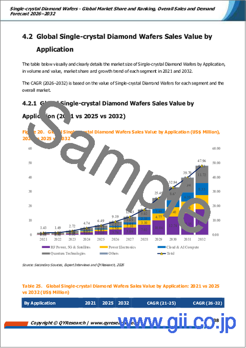
The global market size for single-crystal diamond wafers is estimated to be USD 6.49 million in 2025 and is projected to grow at a CAGR of 31.71% from 2026 to 2032, reaching USD 47.96 million.
The North American single-crystal diamond wafer market was valued at USD 3.71 million in 2025 and is projected to grow at a CAGR of 34.24% from 2026 to 2032, reaching USD 31.78 million by 2032.
The European single-crystal diamond wafer market was valued at USD 0.99 million in 2025 and is projected to grow at a CAGR of 25.52% from 2026 to 2032, reaching USD 5.28 million by 2032.
The Japanese single-crystal diamond wafer market was valued at USD 1.34 million in 2025 and is projected to grow at a CAGR of 26.19% from 2026 to 2032, reaching USD 7.35 million by 2032.
The Chinese single-crystal diamond wafer market was valued at USD 0.31 million in 2025 and is projected to grow at a CAGR of 39.69% from 2026 to 2032, reaching USD 3.12 million by 2032.
Major global companies in the single-crystal diamond wafer market include Orbray, Diamond Foundry Inc, Element Six/E6, EDP Corporation, Advent Diamond, Coherent, Compound Semiconductor (Xiamen) Technology, and Great Lakes Crystal Technologies (GLCT). In 2025, the top three companies accounted for approximately 72% of revenue. Single-crystal diamond (SCD) wafers are still in the early stages of commercialization, and the number of companies entering this field is increasing. Potential new entrants include Diamfab, WD Advanced Materials (WDAM), HiQuTe Diamond, Applied Diamond Inc, Chongqing Origin Stone Element Science and Technology Development, and Ningbo Crysdiam Technology.
This report provides a comprehensive analysis of the global market for single-crystal diamond wafers, covering total sales volume, revenue, price, market share and ranking of key companies, along with analysis by region/country, size, and application.
Market size, estimates, and forecasts for single-crystal diamond wafers are presented in terms of sales volume (units) and revenue (USD million), with 2025 as the base year, including historical data from 2021 and forecast data to 2032. This report combines quantitative and qualitative analysis to assist readers in developing growth strategies, evaluating competitive landscapes, understanding their own position in the current marketplace, and making informed business decisions regarding single-crystal diamond wafers.
Orbray
Diamond Foundry Inc
Element Six (E6)
EDP Corporation
Advent Diamond
Coherent
Compound Semiconductor (Xiamen) Technology
Great Lakes Crystal Technologies (GLCT)
Potential entrants include:
Diamfab
WD Advanced Materials (WDAM)
HiQuTe Diamond
Applied Diamond Inc
Chongqing Origin Stone Element Science and Technology Development
Ningbo Crysdiam Technology
2-inch (50 mm)
3-inch (75 mm)
4-inch (100mm)
Less than 2-inch
RF Power, 5G and Satellite
Power Electronics
Cloud and AI Computing
Quantum Technology
Others
North America
Europe
China
Japan
Others